The board dimension can easily be specified as shown in the following image: Now select the "board edge" layer form the left bottom layer selecting drop down menu.

How to design PCB in Proteus in 10 Minutes +5v Power
Without working schematics, there is a waste of time on designing the pcb board because the pcb board will not work.
How to design pcb in proteus. Here we will use 35. Go to "output" and then "export graphics." select "export adobe pdf file." a new window will appear. In this type mostly smd components are used.
Hit on "save" and save the file in the same place where you saved the initial circuit design. Select the rectangle from the left side menu. Change the "mode" option to "artwork." step 2
This will be your pcb board dimensions. Making sure that there are safe clearances between objects on the pcb is a top priority. After that, you click next.
Ad find reviews, prices, numbers and addresses for the top 10 voted. This will split the component into its. Select 'track mode' and you can change the track width by selecting 'c' (create) or 'e' (edit) as shown.
The beginner level software is the proteus for schematic designing and pcb designing. Click "create a pcb layout from the selected template", and then select arduino uno rev3. It is very simple and easy to understand for beginners in microcontroller programming.
Open the pcb layout you designed using proteus. How to design pcb in proteus 8. You can also make pcb directly but i recommend that use proteus isis first, its quite the easy approach as you don't need to do anything in it and the software intelligence helps you throughout the designing.
After selecting the board edge layer, draw a rectangle around your pcb art work. Printed circuit board design with proteus isis is a very interesting course for hardware developers, microcontroller programmers, embedded system designers, final year students in engineering and technology hobbyist who love to accomplish projects by themselves. Coming to duel layer pcb, tracking is done in two sides and components are placed in two sides also.
Learn to design printed circuit board with proteus | pcb design. Since this is hobbyist pcb made at home, we will use a width greater than 25. Adding jumper wire in pcb design in proteus to draw the jumper wire, you start routing and where you want to place the jumper wire you'll double click and again double click to end the jumper wire.
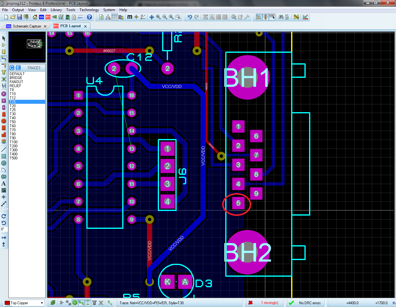
In this two are top and bottom layers and remaining all are inner layers. Select your width according to the pcb you design. Click on p button it stands for place, a new window would appear, in this window you can search for the components by typing exact names like 1n4007(diode) or simply type diode but if you want to make pcb you have to check that your selected component has a pcb design which is shown in pcb preview.
After you click next, an arduino uno layout will appear. In order to design the pcb in proteus ares, first you need to make the circuit of that pcb in proteus isis. Modern electronic products are more complex than ever before, operating at higher speeds and needing to fit into smaller enclosures;
So, let's see how the schematics should be designed and then we will move onto the pcb layout and then board designing. Proteus has the arduino layout as per default. Double click the required component and it would appear in your devices and.
Next, connect all the components. Here's the list of top 10 pcb design software. In order to design the printed circuit board we first need to specify the board dimension of the pcb design in proteus.
A very detailed and easiest method is shown for pcb d. After we have specified the board size of the printed circuit board let us place all the components of the schematics onto the board. Getting pcb output from proteus
This video shows how to create a simple pcb in proteus eda software from schematic capture through to completion of pcb layout as of version 8.6ref: In this course we are going to cover all the necessary aspect to design a high quality printed circuit board. Go to the pcb editor(i think it was ares) and create a user library from the libraries menu.
Completed pcb design of led flasher circuit. This means we need more control over electrical clearances during board layout. Next you can place the footprint from a similar package and right click on it and click decompose(or something similar i can't remember the exact name).
Selecting these buttons will open a new window. In this video pcb design tutorial is given using proteus ares software. Pcb designs near you here!
In proteus we can design up to 16 layers pcb. To do that you need to create a library in proteus. Next finally multi layered pcb's, in these many layers are used.
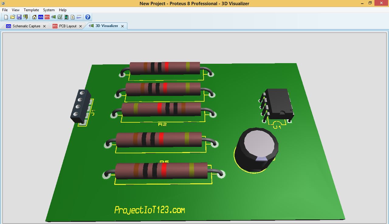
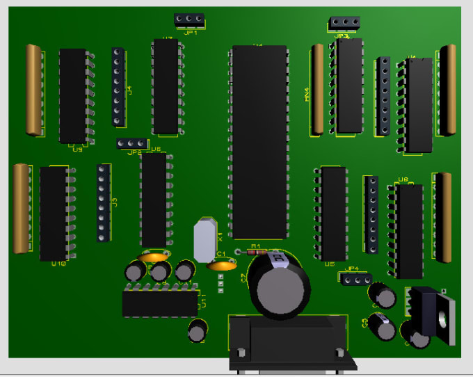
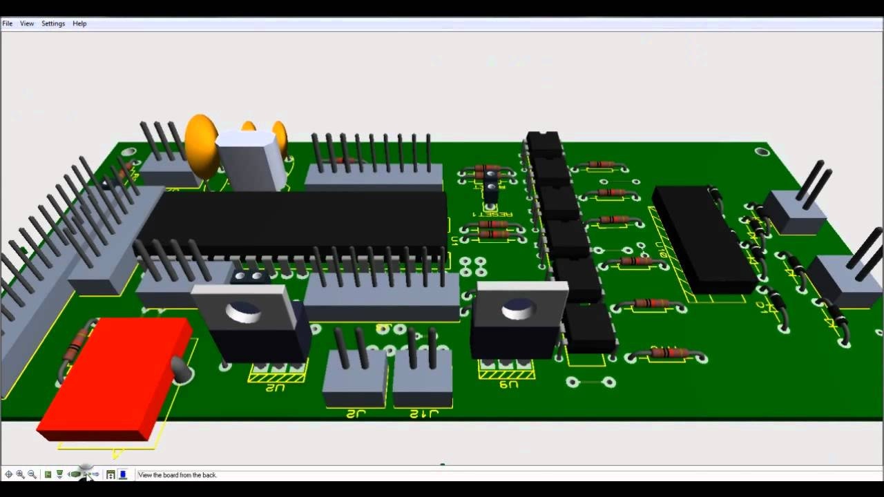
PCB Design in Proteus projectiot123 Technology

Proteus pcb design tutorial

Proteus PCB Design Download [25.8 MB]
Proteus circuit design,simulation,pcb layout by Talha_qureshi_

Reusing Schematic and PCB layouts in Proteus Design Suite

Proteus PCB Design Software Level 3 (Unlimited Pins

Proteus PCB Design Download [25.8 MB]
How To Make Pcb Layout In Proteus PCB Circuits

PROTEUS PCB DESIGN
PCB design with Proteus ISIS guide for Beginners

How to make PCB design by Proteus Software YouTube

Proteus Pcb Design Tutorial Video PCB Circuits
How to design a PCB layout and Circuit digram on Proteus

How To Design PCB on Proteus step by step Guide Urdu
Download Proteus Professional 8.6 Free ALL PC World


Proteus pcb design tutorial

How to create PCB with Proteus single sided PCB design
Help for pcb layout in Proteus 8 Forum for Electronics

Download Proteus PCB Design 8.11 SP0 Build 30052 Free


